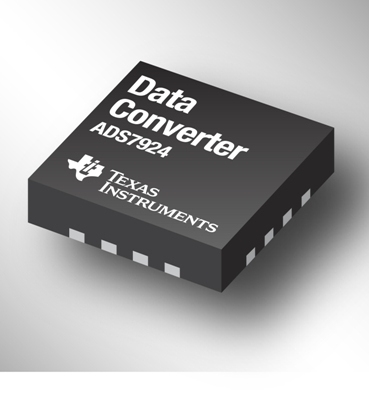
TI ADS548x 16位LVDS ADC方案
TI 公司的ADS5481/ADS5482/ADS5483 (ADS548x)是16位模数转换器(ADC),工作电压5V和3.3V,并提供LVDS兼容的数字输出. ADS548x系列集成了输入缓冲放大器,从而隔离了取样保持和信号源,提供了高阻抗输入.内置的基准电压源简化了系统设计,广泛用在无线基础设备如多载波GSM,WCDMA和LTE,测试和测量仪表以及软件定义无线电(SDR).本文介绍了ADS548x系列的主要特性, 方框图, 模拟输入电路, 时钟输入电路以及最佳抖动时钟电路.The ADS5481/ADS5482/ADS5483 (ADS548x) is a 16-bit family of analog-to-digital converters (ADCs) that operate from both a 5-V supply and 3.3-V supply while providing LVDS-compatible digital outputs. The ADS548x integrated analog input buffer isolates the internal switching of the onboard track and hold (T&H) from disturbing the signal source while providing a high-impedance input. An internal reference generator is also provided to simplify the system design.
Designed for highest total ENOB, the ADS548x family has outstanding low noise performance and spurious-free dynamic range.
The ADS548x is available in a QFN-64 PowerPAD package. The device is built on Texas Instruments complementary bipolar process (BiCom3) and is specified over the full industrial temperature range (–40°C to +85°C).

ADS548x 主要特性:
80/105/135-MSPS Sample Rates
16-Bit Resolution
SFDR = 95 dBc at 70 MHz and 135 MSPS
SNR = 78.6 dBFS at 70 MHz and 135 MSPS
LVDS-Compatible Outputs
Internal Dither Available
Total Power Dissipation: 2.2 W
Powerdown Mode: 70 mW
On-Chip High Impedance Analog Buffer
QFN-64 PowerPAD Package
(9 mm × 9 mm footprint)
Industrial Temperature Range:
-40°C to +85°C
应用:
Wireless Infrastructure (Multi-Carrier GSM, WCDMA, LTE)
Test and Measurement Instrumentation
Software-Defined Radio
Data Acquisition
Power Amplifier Linearization
Communication Instrumentation
Radar
Medical Imaging
相关推荐
TI推出具备智能系统电源管理功能的SAR ADC
2010-07-19
在线研讨会
焦点
