On Semi 255W ATX电源参考设计方案
OnSemi(安森美)公司的255WATX电源参考设计方案具有80PLUS认证的开放式设计,在50%负载和230V与240Vac时效率高达90%,而在50%负载和100V与115Vac时效率大于88%。本文介绍了该参考设计的详细性能,包括ATX电源参考设计简化方框图和详细电路图以及各个部分的材料清单,包括主板(PFC级,同步整流输出级)材料清单,DC-DC转换器级和监视级材料清单,HB谐振LLC级材料清单等。High-Efficiency 255 W ATX Power Supply Reference Design
ON Semiconductor was the first semiconductor company to provide an 80 PLUS-certified open reference design for an ATX power supply in 2005. A second generation 80 PLUS-certified open reference design with improved efficiency was then introduced in 2007.
ON Semiconductor is now introducing its third generation 80 PLUS-certified open reference design with a drastic efficiency improvement. This is a 255 W multi-output power supply for the ATX form factor. Achieving a maximum efficiency of 90% at 50% load, and at 230 and 240 Vac, this third generation reference design achieves >88% efficiency at 50% load, and 100 and 115 Vac.
All efficiency measurements were obtained at the end of a 41 cm (16 in.) cable, ensuring the design can be used ‘as is’ in all standard desktop PC configurations.
This reference document provides the details behind this third generation design. The design manual provides a detailed view of the performance achieved with this design in terms of efficiency, performance, thermals and other key parameters. In addition, a detailed list of the bill-of-materials (BOM) is also provided. ON Semiconductor will also be able to provide technical support to help our customers design and manufacture a similar ATX power supply customized to meet their specific requirements.
The results achieved in this third generation design were possible due to the use of advanced new components from ON Semiconductor. These new ICs not only speeded up the overall development cycle for this new design, but also helped achieve the high efficiencies while at the same time keeping a check on the overall cost.
This third generation design consists of a single PCB designed to fit into the standard ATX enclosure along with a fan. Figure 1 below presents the overall architecture employed in this design. Detailed schematics are included later in this design manual.
The design closely follows the ATX12V version 2.2 power supply guidelines and specifications available from www.formfactors.org, unless otherwise noted. This 255 W reference design exceeds the 80 PLUS Silver (www.80plus.org), ENERGY STAR® 5.0 (www.energystar.gov), and Climate Savers Computing Initiative (CSCI) Step 3 (www.climatesaverscomputing.org) efficiency targets for desktop PC multi-output power supplies. Table 1 hereafter shows a summary of the efficiency targets from these different organizations.

表1.效率目标表

图1.ATX电源参考设计简化方框图

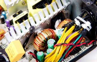
图2.255W ATX电源参考设计外形图

图3. ATX电源参考设计电路图
The bill of materials (BOM) for the design


表2.主板(PFC级, 同步整流输出级)材料清单


表3.DC-DC 转换器级和监视级材料清单

表4.HB 谐振LLC级材料清单

表5.机械和其它材料清单
相关推荐
超安静低功耗 评金达ATX-600T静音版电源
2011-09-21
在线研讨会
焦点