TI PGA308模拟传感器信号调理方案
TI公司的PGA308是可编程的模拟传感器信号调理控制器,能放大传感器信号和数字校准失调和增益.校准通过数字的One-Wire, UART兼容的接口进行.片内有七组OTP存储器,用来存储增益和失调校准参数.器件工作电压从+2.7V 到+5.5V.主要应用在桥式传感器,遥控4-20mA发送器,应力,负荷和称重仪以北及汽车电子传感器.本文介绍了PGA308的主要特性, 详细方框图, 典型的三线应用电路,测试板方框图以及PGA308EVM评估板方框图, 电路图和评估板材料清单.The PGA308 is a programmable analog sensor signal conditioner. The analog signal path amplifies the sensor signal and provides digital calibration for offset and gain. Calibration is done via the 1W pin, a digital One-Wire, UART-compatible interface. For three-terminal sensor modules, 1W may be connected to VOUT and the assembly programmed through the VOUT pin. Gain and offset calibration parameters are stored onboard in seven banks of one-time programmable (OTP) memory. The power-on reset (POR) OTP bank may be programmed a total of four times.
The all-analog signal path contains a 2x2 input multiplexer (mux) to allow electronic sensor lead swapping, a coarse offset adjust, an auto-zero programmable gain instrumentation amplifier (PGA), a fine gain adjust, a fine offset adjust, and a programmable gain output amplifier. Fault monitor circuitry detects and signals sensor burnout, overload, and system fault conditions. Over/under-scale limits provide additional means for system level diagnostics. The dual-use DOUT/VCLAMP pin can be used as a programmable digital output or as a VOUT over-voltage clamp.
PGA308主要特性:
Digital Calibration for Bridge Sensors
Offset Select: Coarse and Fine
Gain Select: Coarse and Fine
Bridge Fault Monitor
Input Mux for Lead Swap
Over/Under Scale Limits
DOUT/ VOUT Clamp Function
Seven Banks OTP Memory
One-Wire Digital UART Interface
Operating Voltage: +2.7V to +5.5V
Temperature Range: -40°C to +125°C
MSOP-10 and 3mm x 4mm DFN-10 Packages
PGA308 主要应用:
Bridge Sensors
Remote 4-20mA Transmitters
Strain, Load, Weigh Scales
Automotive Sensors

图1.PGA308详细方框图

图2.PGA308简化方框图

图3.PGA308典型的三线应用电路
PGA308EVM评估板
The PGA308EVM key hardware consists of two boards, PGA308 Test Board and USB DAQ Platform. The PGA308 Test Board contains the PGA308, terminal strips for external connections, several jumpers for device configuration, and support circuitry. The PGA308 Test Board can be used to fully test your design before prototyping it. The USB DAQ Platform contains an 8052 microcontroller with a built in USB interface. The microcontroller generates the one-wire signals necessary to communicate with the PGA308. The USB DAQ Platform also contains, a 3V/5V programmable linear regulator, a switch for power control, general purpose digital I/O, DAC outputs, and A/D inputs.
block diagram of the PGA308 test board. The PGA308 test board functionality is relatively simple. It provides connections to the one-wire interface, digital-to-analog converter (DAC), analog-to-digital converter (ADC), and general-purpose inputs/outputs (GPIOs) on the USB DAQ platform. It also provides connection points for external connection of the bridge sensor, reference, and outputs.

图4.PGA308测试板方框图

图5.USB DAQ平台方框图

图6.PGA308评估板电路图
PGA308评估板材料清单(BOM):


相关推荐
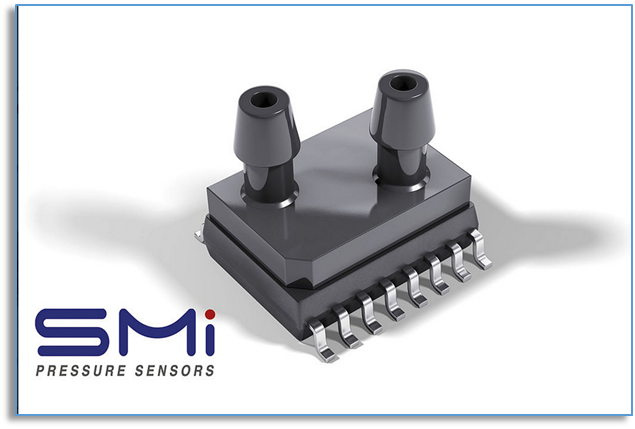
SMI推出高精度、超低量程的压力传感器
产品与技术
2019-07-24
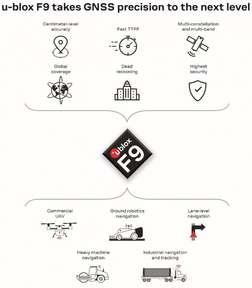
u-blox发表工业与汽车应用的u-blox F9强固型多用途高精度定位技术
产品与技术
2018-02-27
在线研讨会
焦点