博通BCM8109多速率10G分路方案
博通(Broadcom)公司的BCM8109是全集成的MSA兼容多速率SONET/ SDH/10GE/FC/FEC接收器,工作速率包括OC-192(9.953Gbps), 10GE(10.3125Gbps), 10GFC(10.315Gbps)或不同的FEC数据速率(10.664/10.709, 11.096,或11.31Gbps). 10.709Gbps, 11.095Gbps, 11.318Gbps或11.352Gbps.内核工作电压1.0V,功耗650mW,可用于OC-192/STM-64/10GbE/FEC发送设备,ADD/DROP复接器,数字交叉连接,ATM交换骨干网,兆兆位和边沿路由器.本文介绍了BCM8109的主要特性,方框图和功能方框图,主要优势和应用.
BCM8109:Multirate 10-Gbps SONET/SDH/10GE/FC/FEC Demultiplexer
The BCM8109 is a fully integrated MSA-compliant multirate SONET/ SDH/10GE/FC/FEC receiver operating at OC-192 (9.953 Gbps), 10GE (10.3125 Gbps), 10GFC (10.315 Gbps), or different FEC (Forward ErrorCorrection) data rates (10.664/10.709, 11.096, or 11.31 Gbps). The BCM8109 provides deserializer, clock and data recovery (CDR), and
loss-of-signal (LOS) detection circuitry and an advanced feature set that includes phase adjustment and adaptive decision threshold adjustment. The BCM8109 provides high-jitter tolerance and low-jitter generation to comply with Optical Internetworking Forum (OIF), IEEE 802.3ae, Telcordia, ANSI, and ITU-T standards.
The BCM8109 reference clock input frequency is user-selectable to the line rate divided by either 16 or 64. The reference clock output and the LVDS receive parallel bus output can be squelched under user control.
The BCM8109 can be powered with a single 1.2V supply or dual 1.2/3.3V supply without any special power supply sequencing requirements.The BCM8109 is a register-based device; settings can be controlled via the Broadcom Serial Control (BSC) interface.
The BCM8109 comes in a 15 mm x 15 mm, 143-pin BGA package.
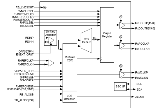
图1.BCM8109方框图
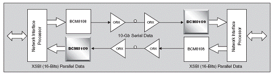
图2. BCM8109功能方框图
主要特性:
10-Gigabit MSA (Multi-Source Agreement) compliant
Fully integrated CDR and demultiplexer with limiting amplifier supports multiple data rates: OC-192, 10GbE, FC, and their FEC data rates.
1:16 DEMUX with LVDS data outputs
Phase adjustment (typical 35-ps range with 2.5-ps granularity)
Adaptive decision threshold level adjustment
Serial data polarity inversion selection
Bit order reversal selection
Lock detect
Exceeds SONET jitter requirements
Core power supply: 1.2V
I/O power supply: CML and LVDS at 1.2V, CMOS at 1.2V or 3.3V
Power consumption: 950 mW
Standard CMOS fabrication process
143-pin BGA package available in standard and Pb-free version
主要优势:
Compliant with Optical Internetworking Forum (OIF), Telcordia®, ITU-T, ANSI, and IEEE 802.3ae industry standards.
Reduces design cycle and time-to-market.
High level of integration allows for higher port density solutions.
Uses the most effective silicon economy of scale for CMOSbased devices.
Low-power consumption eliminates the need for external cooling sources.
应用:
OC-192/STM-64/10GE transmission equipment
SONET/SDH optical modules
ADD/DROP multiplexers
Digital cross-connects
ATM switch backbones
SONET test equipment
Terabit routers
Edge routers
BCM8109:Multirate 10-Gbps SONET/SDH/10GE/FC/FEC Demultiplexer
The BCM8109 is a fully integrated MSA-compliant multirate SONET/ SDH/10GE/FC/FEC receiver operating at OC-192 (9.953 Gbps), 10GE (10.3125 Gbps), 10GFC (10.315 Gbps), or different FEC (Forward ErrorCorrection) data rates (10.664/10.709, 11.096, or 11.31 Gbps). The BCM8109 provides deserializer, clock and data recovery (CDR), and
loss-of-signal (LOS) detection circuitry and an advanced feature set that includes phase adjustment and adaptive decision threshold adjustment. The BCM8109 provides high-jitter tolerance and low-jitter generation to comply with Optical Internetworking Forum (OIF), IEEE 802.3ae, Telcordia, ANSI, and ITU-T standards.
The BCM8109 reference clock input frequency is user-selectable to the line rate divided by either 16 or 64. The reference clock output and the LVDS receive parallel bus output can be squelched under user control.
The BCM8109 can be powered with a single 1.2V supply or dual 1.2/3.3V supply without any special power supply sequencing requirements.The BCM8109 is a register-based device; settings can be controlled via the Broadcom Serial Control (BSC) interface.
The BCM8109 comes in a 15 mm x 15 mm, 143-pin BGA package.
图1.BCM8109方框图
图2. BCM8109功能方框图
主要特性:
10-Gigabit MSA (Multi-Source Agreement) compliant
Fully integrated CDR and demultiplexer with limiting amplifier supports multiple data rates: OC-192, 10GbE, FC, and their FEC data rates.
1:16 DEMUX with LVDS data outputs
Phase adjustment (typical 35-ps range with 2.5-ps granularity)
Adaptive decision threshold level adjustment
Serial data polarity inversion selection
Bit order reversal selection
Lock detect
Exceeds SONET jitter requirements
Core power supply: 1.2V
I/O power supply: CML and LVDS at 1.2V, CMOS at 1.2V or 3.3V
Power consumption: 950 mW
Standard CMOS fabrication process
143-pin BGA package available in standard and Pb-free version
主要优势:
Compliant with Optical Internetworking Forum (OIF), Telcordia®, ITU-T, ANSI, and IEEE 802.3ae industry standards.
Reduces design cycle and time-to-market.
High level of integration allows for higher port density solutions.
Uses the most effective silicon economy of scale for CMOSbased devices.
Low-power consumption eliminates the need for external cooling sources.
应用:
OC-192/STM-64/10GE transmission equipment
SONET/SDH optical modules
ADD/DROP multiplexers
Digital cross-connects
ATM switch backbones
SONET test equipment
Terabit routers
Edge routers
相关推荐
在线研讨会
焦点